Humanoid Robot
This is the major work I did at STMicroelectronics, which aims to promote new technologies based on the ST ecosystem.
As a System Application Engineer at ST, I focus on developing solutions for the Smart Industrial area using ST products.
One key area we have recently focused on is the Humanoid Robot, Joint Module, Robotic Hands, and Sensors.
Joint Module
Humanoid robotics is entering a scale-up phase, and the joint module is one of the most decisive parts for performance, cost, and reliability. A single humanoid robot typically requires dozens of joint modules distributed across the neck, shoulders, elbows, wrists, hips, knees, and ankles—making the total addressable market substantial and structurally long-term as volumes grow and platforms iterate.
More importantly, a “joint module” is not a simple motor. It is a tightly integrated mechatronic system that combines a high-torque density motor, a precision reducer (often a harmonic drive), dual encoders (rotor and output-axis) for commutation and absolute positioning, a brake for safe holding, and frequently a torque sensor for compliant control—along with the embedded servo drive electronics that must manage power conversion, sensing, protection, real-time control, and communication in a compact, thermally constrained package. This architecture makes joint modules complex to engineer, difficult to manufacture at scale, and highly sensitive to design trade-offs in efficiency, accuracy, noise, and safety.
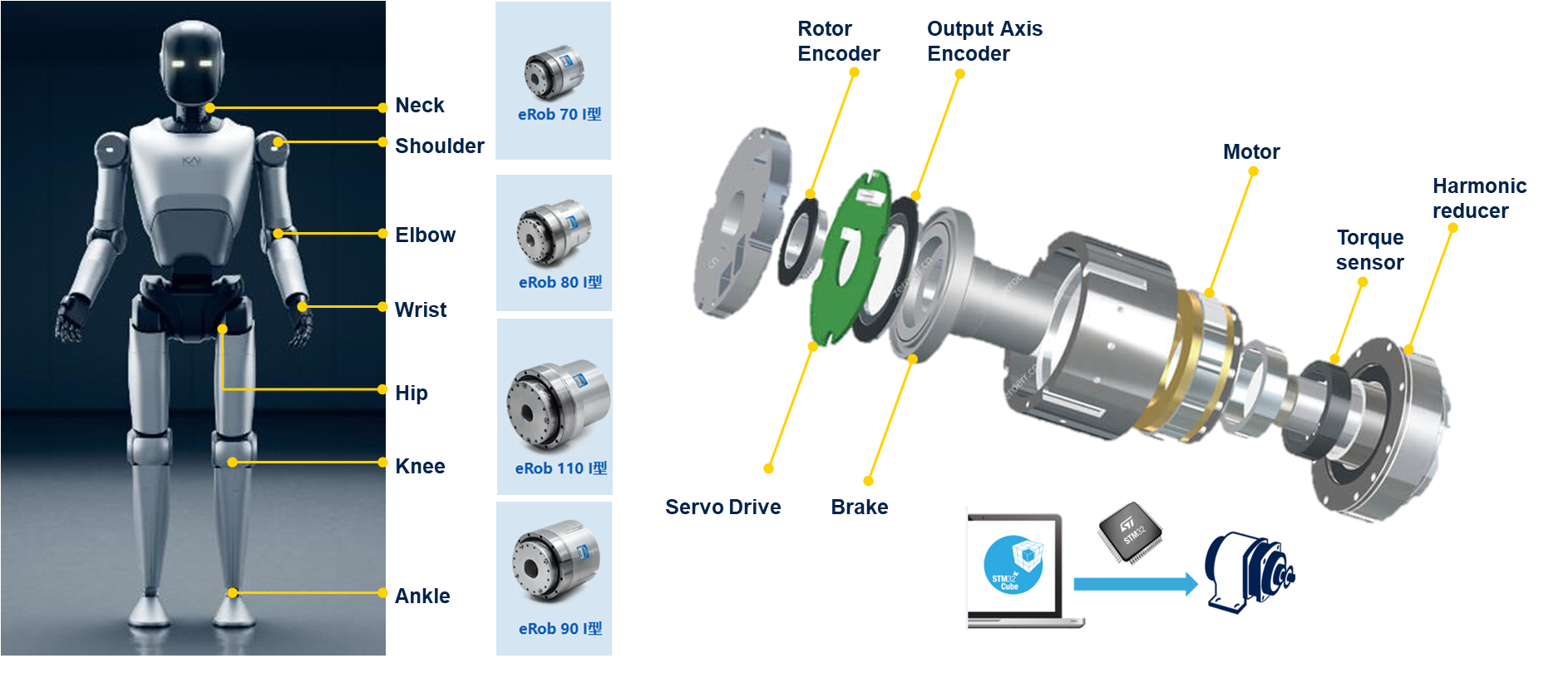
Our primary focus is the servo drive (drive board) inside the joint module—delivering high-performance motor control electronics and firmware that enable stable torque/position control, robust protection, and scalable integration for next-generation humanoid actuators.
Performance Index
- High torque density
- High efficiency (> 90 %)
- Fast dynamic response (< 1 ms latency)
- Precise position & torque control (< 0.1° error)
- Compact size & lightweight
- Integrated FOC driver (current loop > 2 kHz)
- Communication: EtherCAT / CAN FD / RS-485
- Protection: OCP / OVP / OTP / UVLO / Short-Circuit
- Environment: IP65, -10 °C ~ 60 °C
What we provide
We provide a motor driver reference solution that includes an STM32, MOSFET, Gate driver, DC-DC, LDO, CAN/RS-485 transceiver, ESD protection, and Op-Amp.
We provide MCSDK, which is a motor control software development kit. It offers quick FOC setup, automatic code generation, and hardware parameter configuration. Compared with Simulink, MCSDK is hardware-oriented and ready for deployment, whereas Simulink is model-oriented and simulation-focused.
Our team focuses on demonstration; we will design our solution based on the existing mechanical structure.
What can we do with GaN HEMTs and STM32G5
- Higher Power Efficiency & Compact Design
- efficiency > 96 % @ 48 V / 300 W (typical efficiency).
- Peak output power up to 3 kW without active cooling (fan-less) — thanks to low switching and conduction losses of GaN HEMTs.
- High power density, Reduced thermal dissipation — compact design
- Optimized PCB layout for low parasitic ensures clean switching and low EMI noise.
- Fast Dynamic Response
- High switching frequency up to 3 MHz → enables ultra-high current-loop bandwidth, improving FOC and torque response.
- Control MCU frequency up to 205 MHz → allows more precise current, velocity, and position control with reduced computational latency.
- Minimal dead-time (< 50 ns) and low switching losses → deliver smoother current waveforms and reduced torque ripple.
- Current loop bandwidth > 5 kHz, enabling millisecond-level torque response for robotic joint control.
Why GaN is better
1) Structural differences → loss differences (with typical share)
Silicon power MOSFET (vertical DMOS/Trench)
- Has P-body + N drift region, with P-body shorted to Source
- This inherently creates a PN body diode (S→D)
- When the body diode conducts forward, minority carriers are injected and stored → reverse-recovery charge (Qrr)
- During commutation, that stored charge must be removed → reverse-recovery loss
GaN e-mode HEMT (lateral AlGaN/GaN heterojunction)
- Main conduction channel is 2DEG (two-dimensional electron gas); reverse conduction is largely channel-based
- No Si-like PN body diode minority-carrier storage; practically (Qrr≈0)
- Hence the “(Qrr) removal” hard-switching penalty is largely eliminated (especially beneficial at high (V)/high (fsw))
Typical reverse-recovery loss share of total loss (rule-of-thumb):
- Low (f) (≤50 kHz), low bus (≤24–48 V): ~5–20% (often lower)
- Mid/high (f) (100–500 kHz) or higher bus (≥48–100 V): ~20–40%
- High (V)/high (f) hard-switching: can reach 40–60%+ (Strongly dependent on (fsw), (Vbus), deadtime, di/dt, and device (Qrr).)
Engineering estimate: \(P_{rr}\approx Q_{rr}\cdot V_{bus}\cdot f_{sw}\cdot N\)
2) PN junction states → why commutation loss is large
For a Si half-bridge / synchronous buck / one inverter leg:
Deadtime/freewheeling: a body diode PN junction becomes forward-biased
- Minority carriers are injected and stored → (Qrr)
Commutation instant: the opposite switch turns on and the switching node slews
- The previously forward-biased PN junction is forced into reverse bias
- Before stored charge is cleared, the diode conducts a reverse-recovery current spike (irr(t))
Why loss is large: the current spike overlaps with high voltage \(E_{rr}=\int v(t),i_{rr}(t),dt \approx Q_{rr}\cdot V_{bus}\)
3) Smaller Miller capacitance → lower gate-drive loss (with formulas)
Gate-drive energy per switching event: \(E_{gate}\approx Q_g\cdot V_{drive}\) Average gate-drive power: \(P_{gate}=Q_g\cdot V_{drive}\cdot f_{sw}\) with (Qg=Qgs+Qgd). The Miller portion (Qgd) is tied to (Cgd) and dominates the voltage-transition plateau.
- Smaller Miller ((Qgd}) / effective (Cgd)) ⇒ smaller (Qg) ⇒ lower (Pgate) at a given (fsw), or higher feasible (fsw) for the same drive-loss budget.
What is the challenge
- Difficult hardware design
- Complex hardware design — requires careful PCB layout and driver design to minimize parasitic inductance.
- Narrow gate voltage margin — sensitive to overshoot; demands precise gate driver control.
- Limited short-circuit robustness — shorter fault-tolerance time compared to Si MOSFETs.
- High dv/dt and EMI sensitivity — fast switching edges increase EMI and layout constraints.
- Application
- Higher BOM cost — GaN devices and dedicated drivers are more expensive.
- Cost-sensitive limitation — less suitable for low-cost applications (e.g., consumer or robotic dog platforms).
Robotic Hands
Overall humanoid robot
Humanoid robot with gesture recognition and voice control
Humanoid robot follow gesture using STM32N6
Past work
In the past, we have developed many solutions for smart homes, especially for KNX. Which is a leading international protocol in smart home automation that ensures seamless compatibility and plug-and-play functionality across devices. We’ve developed various demos to showcase the integration of ST’s products. During the development process of those demo solutions, I got more familiar with ST products, such as STM32 MCU/MPU, chips, KNX protocol chips, IO-Link protocol chips, edge AI sensors, DC-DC converters, and energy harvesting chips. Our demos include smart charging stations, mini IoT houses, photovoltaic energy storage and harvesting, IoT sensors, KNX-based smart building management systems, and solutions for remote network monitoring and intranet penetration.